STUDY OF LOGIC GATES INTEGRATED CHIPS CONNECTION PROCEDURE
The truth tables of {AND} {OR} {NOT} Gates using integrated IC [ integrated chips ]
Components Required:
Digital Logic Trainer kit
IC [ #7408,7432,7404 ]
[AND] [OR] [NOT] Connecting Wires and Power Supply.
1.) Verification of [ AND gate ]
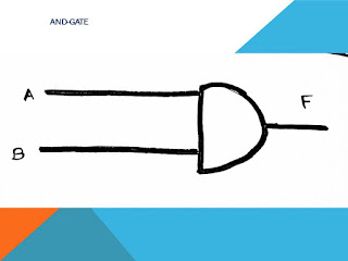
Gate Symbol:
Logic Function[ F= A.B ]
Rules:
- If both the inputs are high(1)result is high(1) other wire the output is low (0)
Truth Table:
|
A |
B |
Y=A.B |
|
0 |
0 |
0 |
|
0 |
1 |
0 |
|
1 |
0 |
0 |
|
1 |
1 |
1 |
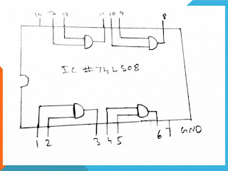
Pin Diagram:
Connection Procedure:
- Insert IC #74LS08 in the Bread Bard.
- Connect pin #7 to Ground and pin #14 to power Supply (+5V).
- Connect pin #1 to First input switch A.
- Connect pin #2 to Second input Switch B.
- Connect pin #3 to any of the output switch Led.
- Switch on the power Supply.
- verify all input possibilities in the truth table.
2.) Verification of [ OR-gate ]:
Gate Symbol
Logic Function [ F=A+B ]
Rule:
- IF any one of the input is high (1) the result in high (1) Otherwise the result is Low (0).
Truth Table:
|
A |
B |
F=A+B |
|
0 |
0 |
0 |
|
0 |
1 |
1 |
|
1 |
0 |
1 |
|
1 |
1 |
1 |
Pin Diagram:
Connection Procedure:
- Insert IC #74LS32 in the Bread Board.
- Connect Pin #7 to Ground and pin #14 to Power Supply(+5v).
- Connect pin #1to First input switch A.
- Connect pin #2 to Second input switch B.
- Connect pin #3 to any one of the output Switch Led.
- Switch [ ON ] Power Supply.
- Verify all input Possibilities in the Truth Table.
3.) Verification of [ NOT gate ]:
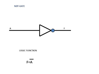
Gate Symbol
Logic Function [ F=A ]
Rule:
- IF the input in low(0) the output is high(1) if the input in high(1) the output is low (0).
Truth Table:
|
A |
A_ |
|
0 |
1 |
|
1 |
0 |
Pin Diagram:
Connection Procedure:
- Insert IC #74LS04 to the Bread Board.
- Connect Pin #7 to ground and pin #14 to Power Supply (+5V).
- Connect pin #1 to first input Switch A.
- Connect pin #2 to any one of the Output Switch Led.
- THE [ ON ] SWITCH THE POWER SUPPLY.
- Verify all the input possibilities in Truth Table.


No comments:
Post a Comment